

2026 Accumulator CAD Model
Formula Electric at Berkeley
–
UC Berkeley
High-Voltage Battery Module Design
Sep 2024 – Ongoing
Overview
Formula Electric at Berkeley designs and builds a complete electric race car from scratch each year to compete in the Formula SAE Electric series. I joined the Accumulator Mechanical subteam in Fall 2024 as the primary designer for the battery modules, the ten lithium-ion segments that together make up the car’s high-voltage battery pack. My work covered the full design process: architecture, mechanical design, structural and thermal analysis, and PCB integration, all developed within a 150-person team collaborating across every system on the car. The modules are currently in fabrication.
Design Goals and Constraints
The 2025 accumulator was designed around three priorities: safety, manufacturability, and high power delivery. Energy density was deliberately secondary, this was a year to validate our fully custom systems before optimizing further.
To maximize motor efficiency, we targeted a peak pack voltage (588V) as close as possible to the competition’s 600V limit. The final configuration is 10 modules in series, each a 14S3P arrangement of Molicel P42A 21700 cells, assembled using ultrasonic wirebonding, a technique we adopted after securing a sponsor with wirebonding capabilities. This meant we could finally move away from the prebuilt parallel cell modules the team had relied on in prior years and design everything from first principles.
FSAE’s rules imposed strict requirements on the design, including rules on high-voltage isolation, overcurrent protection, cell restraint under crash-level acceleration loads, and temperature monitoring placement. Each of these directly shaped the design.

2026 Module Exploded View
Module Architecture
To restrain the cells at the top, I proposed a design which used the voltage sensing PCB itself as a structural plate. This board, which I designed in CAD in collaboration with the EECS team, sits directly on top of the cell array. It has precision-cut holes that fit around each cell and thick copper pads on its surface that the wirebonding machine bonds directly to, making the cell-to-cell electrical connections. Because it spans the full footprint of the module and is fastened to the structure on its short edges, it also acts as the plate that keeps the cells from moving upward under load. One part doing two jobs, drastically lowering our part count, and simplifying our manufacturing efforts substantially. This change removed multiple machining operations on the cell restraints that would have been necessary otherwise.
The wirebonding process is worth explaining briefly because it is what makes this module design possible. Instead of spot-welding tabs between cells like many custom battery packs, ultrasonic wirebonding uses a CNC mahcine to draw a thin copper wire across the surface of each cell terminal and bonds it in place using high-frequency vibration. Each wire is thin enough to act as its own fuse, called a fusible link. If a cell fails and draws too much current, its fusible inks melt open and isolate it from the rest of the pack. The beauty of this approach is that the high precision connections allow both the positive and negative connections to be made on one surface of the battery cell. The positive bond is made directly to the terminal on the top of the cell. The negative bond is made to the rim of the cell, where the heat shrink has been trimmed back a few mm to expose the negative rim of the can. This leaves the bottom surface of the cell completely free, where we monitor cell temperatures.
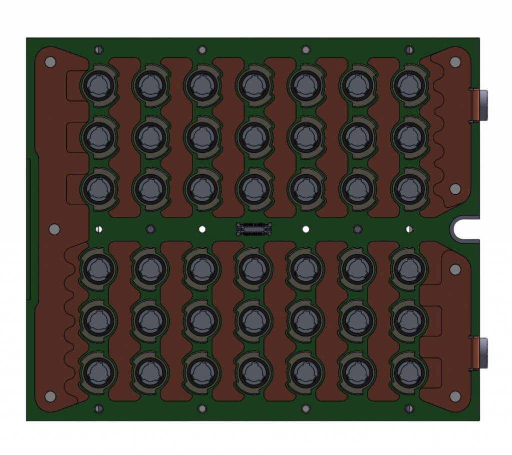
Cell and Busbar Layout + Voltage Sense PCB
On the bottom of the module, a custom temperature sensing PCB sits in contact with the exposed negative terminal of each cell, monitoring temperatures individually across all 42 cells. A third board, the BMS PCB, sits atop the VSense and plugs into the other two via board-to-board connectors and ribbon cables. This BMS board handles cell voltage monitoring, safety shutoff logic, and inter-module communication. This three-board stack was my proposal. The key advantage is that the BMS board is fully hot-swappable: the EECS teams can disconnect it and make firmware or hardware changes without getting anywhere near the high-voltage cell connections, which are covered by the other two boards and their protective covers.
Every high-voltage surface in the module is covered by two independent layers of protection. The inner layer covers the cell connections and busbars. An outer polycarbonate cover protects the PCBs and can be removed for maintenance without exposing any cells or live connections underneath. The module is designed so that the only conductive surfaces exposed on the exterior are the terminals themselves. All exterior-facing hardware is nylon to ensure nothing conductive is reachable from outside the module.
The module enclosure uses polycarbonate as its primary structural material, with 3D printed UL94-V0 rated spacers throughout. Finding a filament that met both the dielectric and flame resistance ratings required by FSAE was one of the more tedious material selection compliance problems, we landed on Bambu Labs FR filament.
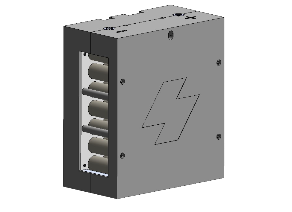
Encased module
Analysis
The VSense PCB structural analysis was the most involved FEA I ran on this project. Because FR4 is a layered composite material, I used anisotropic FEA techniques to model it in SolidWorks, which required manual material design in the software. The failure mode, cracking or cells coming loose inside a live high-voltage pack, was serious, as reflected by FSAE’s requirement that cell restraining parts must be able to withstand an acceleration of 40g in every direction. To ensure our novel approach to cell restraint would be compliant, I ran these FEAs many times on variable PCB thicknesses to determine preciesly what spec of material was necessary to keep both deflection and factor of safety within our tolerances. That analysis drove the selection of 3mm as our PCB thickness. I repeated this FEA a few times as other parts of the assembly became finalized, including the full screw pattern and all structural components, confirming the assembly as a whole stays well below yield.

VSense Cell Retention FEA
Because we use wirebonds as fusible links for per-cell overcurrent protection, FSAE rule EV.6.6.5 requires that they be formally rated, either with manufacturer data or with test data we generate ourselves. No data existed for our specific wire dimensions and bond parameters, so I designed a rule compliant testing program to collect it. The setup passes variable high current through individual fusible links using a high-power low-voltage source to hit target current levels. To measure current and fuse time through links of varying wire diameter, bond length, and material, voltage across a shunt resistor is sampled at over 200 Hz to capture the full current waveform and time to fuse. FSAE requires a minimum of four trials at each of at least four current levels for the data to qualify. I documented the full experiment design, instrumentation requirements, safety protocols, test fixture design, and data recording procedure in a detailed DOE and SOP so that team members could execute the testing independently. The team is currently running those tests.
FSAE rules require thermistors to be in direct contact with the cell they are monitoring, or to demonstrate equivalent thermal coupling through whatever interface material separates them. This posed a problem for our design: the thermistors are on a low-voltage PCB, so they need to be electrically isolated from the cells, which are live high-voltage surfaces. Placing an insulating material between the thermistor and the cell was necessary for safety, but we had to prove that material would not meaningfully slow the thermistor’s thermal response. I ran a 1D transient heat conduction simulation in MATLAB, modeling a step change in cell surface temperature and solving for the temperature at the thermistor over time across different material thicknesses and thermal conductivities. These simulations were the basis for selecting a specific thermal gap filler interface material that met all four of our constraints simultaneously: thermal conductivity fast enough to satisfy the FSAE direct-contact equivalency requirement, sufficient dielectric strength to electrically isolate the PCB from the cells, and physical properties compatible with our fabrication and assembly process.

Heat Conduction FEA
Parametric Modeling
The module assembly has over 200 components across multiple subassemblies. I built it around a master sketch driven by global dimensions in SolidWorks, so that high-level parameters such as cell spacing, busbar thickness, module length, and screw placement propagate through the entire model automatically. This made iteration fast, kept the design consistent across subassemblies, and made it straightforward to hand off to the people building it. I was thinking about manufacturability from the first sketch: every mechanical part was chosen or designed with in-house fabrication in mind, using materials and processes available to the team.
Collaboration
The modules subteam had four members, within a 14-person Accumulator Mechanics group and a 150-person team overall. I took primary ownership of the CAD and analysis, but the design was genuinely a group effort. I worked closely with the cooling subteam on thermal integration and cell spacing, with the EECS team on PCB geometry and connector placement, and with the full accumulator group in regular design reviews to integrate the modules into the broader car assembly. The modules are currently in fabrication and I am still in regular contact with the team to support assembly.
What I Took Away
This project pushed me to think carefully about how mechanical, electrical, and thermal systems intersect inside a tightly constrained package. The problems I found most interesting weren’t the ones with obvious solutions — they were the ones where the right answer required understanding the constraints from multiple disciplines at once. That’s the kind of engineering I want to keep doing.